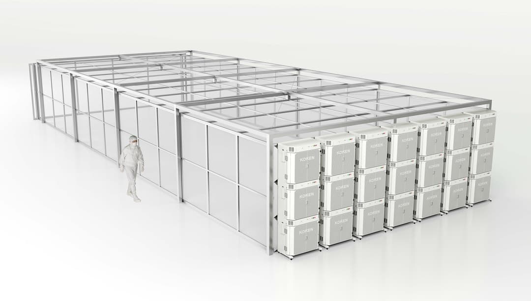
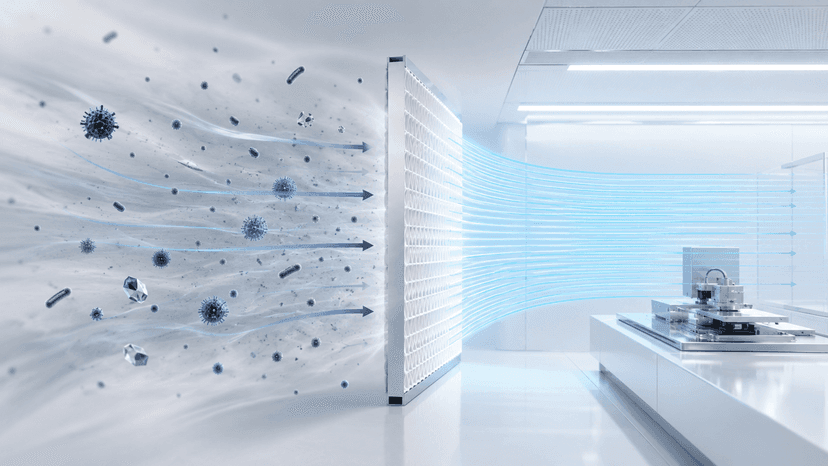
Evaluation and analysis play a major role in developing sustainable materials for industries. HORIBA contributes to identifying and overcoming climate challenges, paving the way for a more sustainable future. The key challenges in materials science involve innovation, traceability, circularity, contributions to climate goals, carbon neutrality, zero pollution, and decarbonization. One of the primary focuses lies in the research and development of new materials, including polymers, metals, composites, biomaterials, carbon materials for energy, and raw materials for semiconductors. Semiconductors and Materials do not exist as distinct markets, but are interconnected, forming a value chain similar to that of textiles. The beginning of this process is Wafer. Each process, like Deposition, Lithography, Etching, and CMP, has a very large value chain. Moreover, the process is supported by huge facilities.
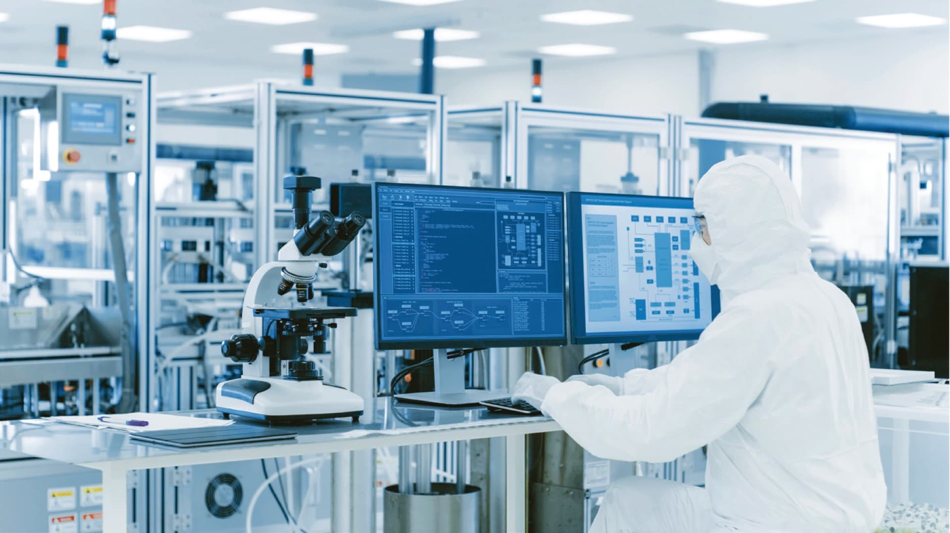
Materials and Semiconductor
Featured Products
Explore our range of high-quality products