HORIBA India at SEMICON India 2025: Enabling the Semiconductor Ecosystem “Lab to Fab”

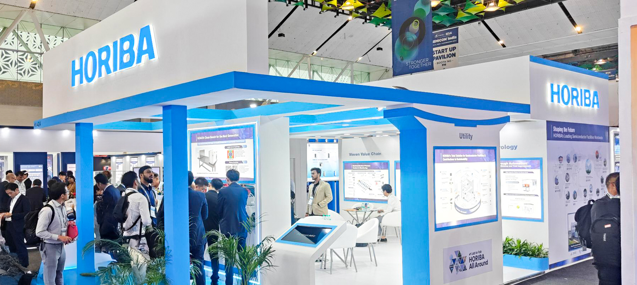
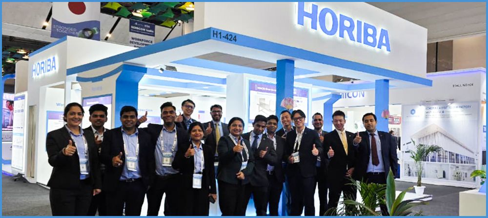
HORIBA India proudly participated in SEMICON India 2025, held from September 2–4 at Yashobhoomi International Convention Centre (IICC), New Delhi. With 35,000+ registrations, 350 exhibitors, and delegates from 48 countries, the event marked a milestone in India’s semiconductor journey.
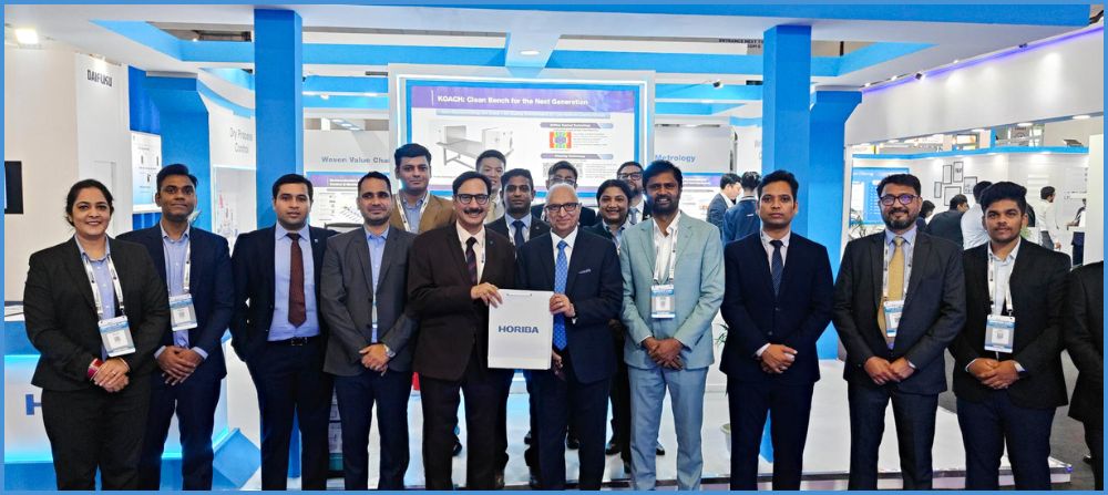
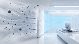
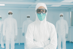
At Booth #424, Hall 1, HORIBA showcased its comprehensive "Lab to Fab" solutions for Deposition, Lithography, Etching, CMP, and Packaging processes. From Mass Flow Controllers and Optical Emission Spectrometers to Residual Gas Analyzers and End Point Gas Monitors, HORIBA demonstrated how Control, Measurement, and Analysis expertise empower researchers, OEMs, and end users across the value chain. The main highlight was the launch of KOACH — a mini clean room that creates an ISO Class 1 local environment, solving airborne particulate contamination challenges in laboratories. Alongside, HORIBA presented its Wafer Inspection System and other advanced process-control tools.
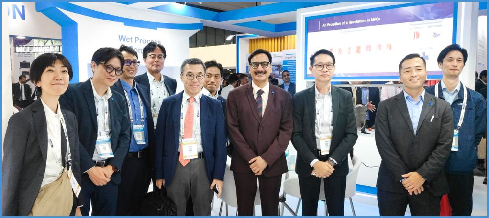
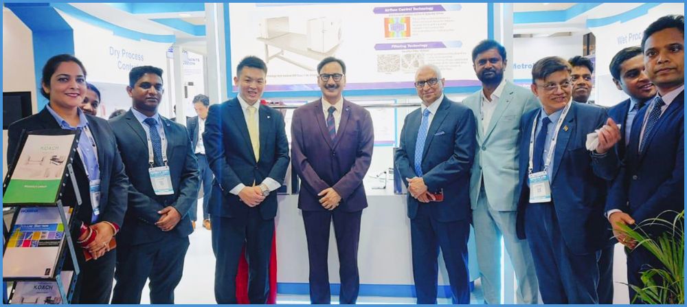
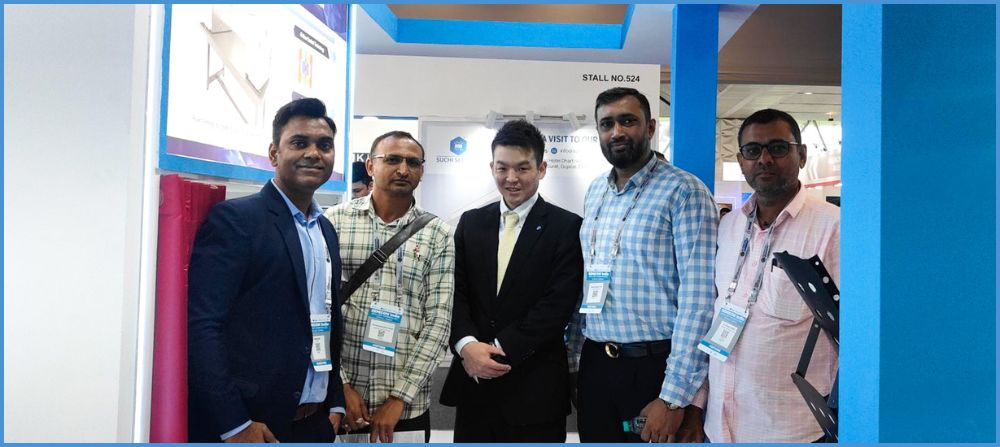
HORIBA also contributed to SEMICON’s inauguration, a key panel session on Materials & Electronics, and multiple industry collaborations, including an MoU with PTW. Strategic meetings with Applied Materials (AMAT), LAM Research, TATA, Indian Institute of Technology (IIT) Delhi, and India Semiconductor Mission (ISM) reinforced our role in enabling India’s semiconductor future. SEMICON India 2025 truly set a new benchmark for collaboration, and HORIBA is proud to be part of this mission, empowering the industry with cutting-edge solutions from Lab to Fab.