
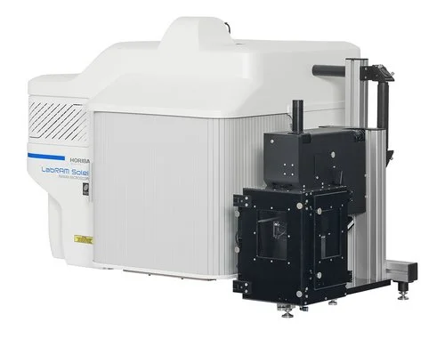
LabRAM Soleil Nano
AFM-Raman Nanoscopy System
LabRAM Soleil Nano is a fully integrated AFM‑Raman nanoscopy system combining HORIBA’s LabRAM Soleil Raman microscope with OmegaScope scanning probe microscopy. It enables co‑localized AFM imaging (topographic, electrical, mechanical) and Raman/photoluminescence spectroscopy, performed sequentially or simultaneously at a single sample location. Tip‑Enhanced Raman Spectroscopy (TERS) and Photoluminescence (TEPL) achieve optical resolution down to 10 nm. Compatible with environmental and low‑temperature chambers, it offers automated operation, high collection efficiency, and ultrafast imaging with SmartSampling™ and Q‑Scan™ modes.
Why Choose LabRAM Soleil Nano
- Real‑time co-localized AFM and Raman/PL measurements at the same sample location
- TERS/TEPL for optical resolution down to 10 nm
- Macro‑to‑nanoscale multimodal analysis on one AFM‑Raman platform
- Fully automated operation enabling results within minutes
- High collection efficiency via top‑down and oblique detection with high‑NA objectives
- Environmental and low‑temperature chamber compatibility for controlled studies

Key Advantages of LabRAM Soleil Nano
Ultrafast mapping
Turns hours of Raman mapping into minutes
Nanoscale optical resolution
Reveals chemical information beyond diffraction limits
Broad multimodal flexibility
Supports Raman, PL, EL and more
Automated robustness
Minimizes setup time and ensures reproducibility
Technical Specifications of LabRAM Soleil Nano
| Specification | Details |
|---|---|
| Sample Scanning Range | 100 µm × 100 µm × 15 µm (±10%) |
| Scanning Non-linearity (XY/Z) | 0.05% XY; 0.05% Z |
| Noise Performance | XY: 0.1 nm RMS (cap sensors ON, 200 Hz); 0.02 nm RMS (OFF, 100 Hz); Z: <0.04 nm RMS (1000 Hz) |
| Resonance Frequency | XY: 7 kHz (unloaded); Z: 15 kHz (unloaded) |
| Movement Control | Digital closed-loop control on X, Y, Z; Motorized Z approach (18 mm) |
| Sample Size | Max 40 × 50 mm, 15 mm thickness |
| Sample Positioning | Motorized range 5 × 5 mm; 1 µm resolution |
AFM Head
| Specification | Details |
|---|---|
| Laser Wavelength | 1300 nm (non-interfering with Raman detector) |
| Noise (Registration System) | < 0.1 nm |
| Alignment | Fully automated cantilever & photodiode alignment |
| Probe Access | Free access for external manipulators and probes |
SPM Measuring Modes
| Modes Supported |
|---|
| Contact AFM (air/liquid) |
| Semicontact AFM (air/liquid) |
| Non-contact AFM |
| Phase Imaging |
| Lateral Force Microscopy (LFM) |
| Force Modulation |
| Conductive AFM (optional) |
| Magnetic Force Microscopy (MFM) |
| Kelvin Probe Force Microscopy (KPFM) |
| Capacitance & Electric Force Microscopy (EFM) |
| Force Curve Measurement |
| Piezo Response Force Microscopy (PFM) |
| Nanolithography |
| Nanomanipulation |
| STM (optional) |
| Photocurrent Mapping (optional) |
| Volt-Ampere Characterization (optional) |
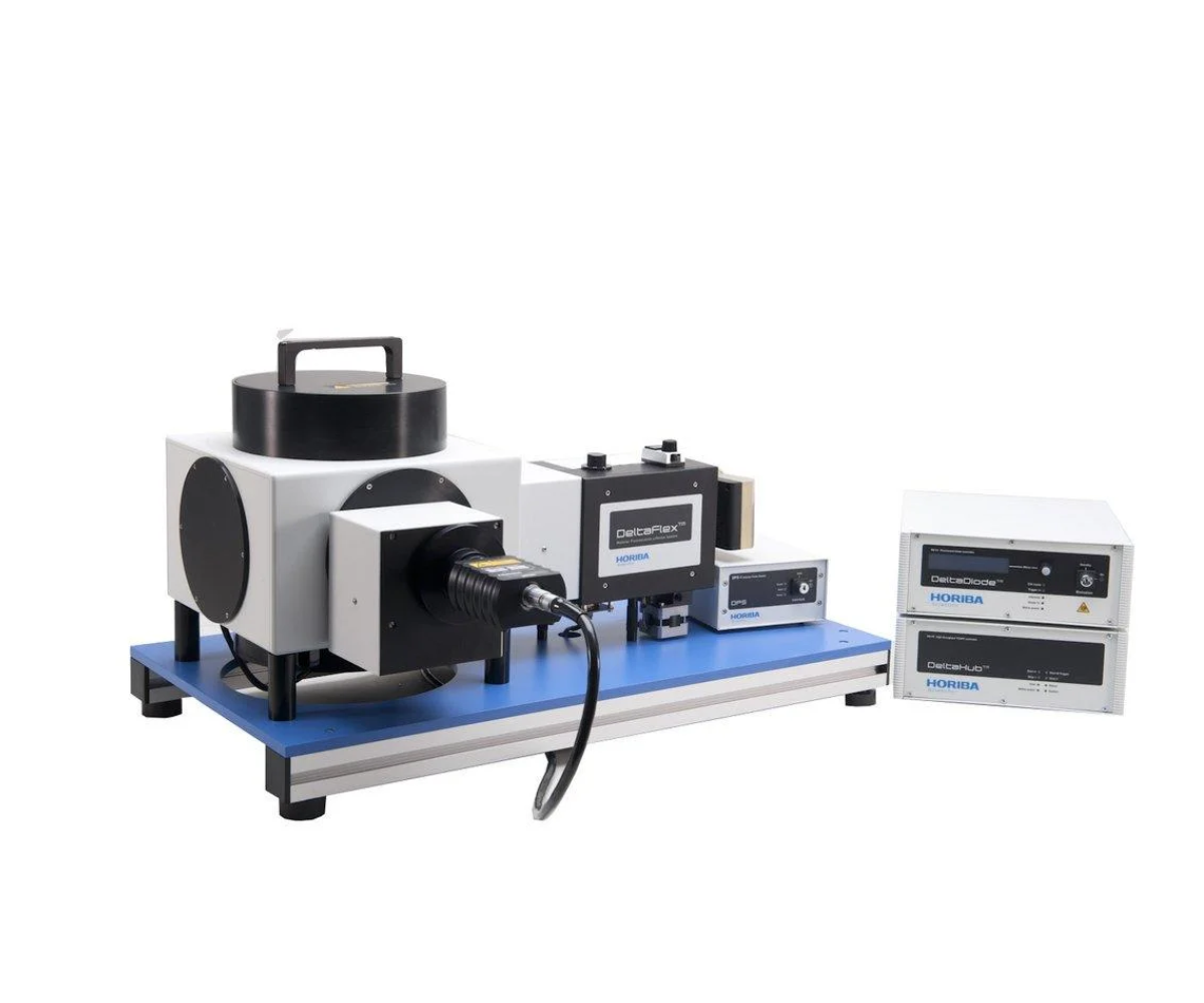
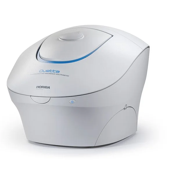
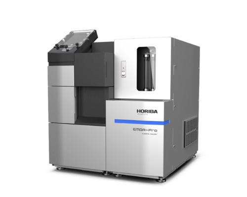
Related Products
NOT SURE WHAT YOU ARE LOOKING FOR?
BOOK A CONSULTATION
Our experts are here to guide you to the right solution. Fill out the form and we'll get in touch shortly.