HORIBA India Showcases Advanced Lab to Fab Solutions at SEMICON India 2026
An exciting start to SEMICON India 2026 as HORIBA India welcomed industry leaders, partners, customers, and innovators to explore the latest advancements in semiconductor process control, particle cha
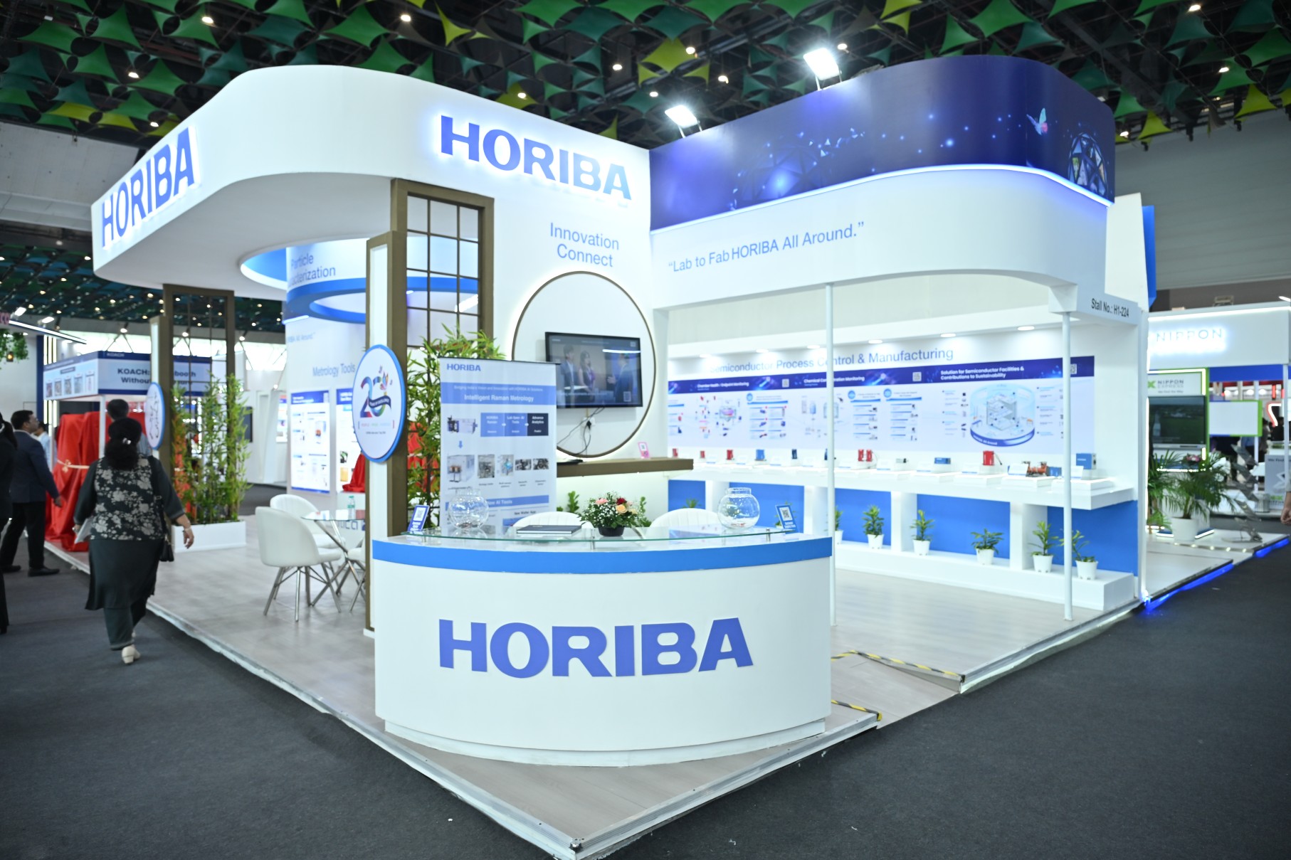
HORIBA India marked an exciting start to its participation at SEMICON India 2026, being held from 17–19 September 2026 at Yashobhoomi (IICC), New Delhi, showcasing a comprehensive portfolio of analytical, measurement, process control and cleanroom solutions for the rapidly evolving semiconductor industry.
At Hall 1, Booth 224, HORIBA is bringing together technologies spanning the semiconductor value chain — from material characterization and process monitoring to fluid control, contamination management, mask inspection and advanced manufacturing environments — demonstrating its capabilities across the journey from “Lab to Fab.”
The participation reinforces HORIBA’s commitment to supporting the development of India’s semiconductor ecosystem through measurement expertise, global technologies and solutions designed for increasingly sophisticated semiconductor manufacturing processes.
Global Leadership Joins HORIBA India at SEMICON India 2026
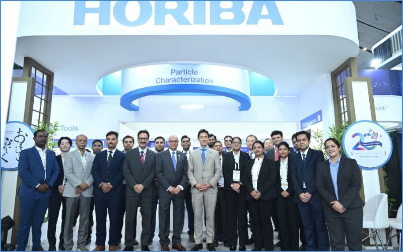
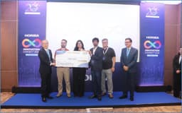
The opening day witnessed participation from HORIBA’s global and India leadership, including Dan HORIBA, Executive Director, HORIBA, Ltd.; Hideyuki Koishi, Chairman, HORIBA India; and Dr. Rajeev Gautam, President, HORIBA India.
Their presence underlined the strategic importance of India within the evolving global semiconductor landscape and HORIBA’s continued focus on contributing technologies, expertise and collaborative capabilities to the country’s semiconductor growth journey.
Throughout the day, the HORIBA team welcomed industry leaders, customers, technology partners, researchers and other stakeholders for discussions around emerging semiconductor manufacturing requirements and the role of advanced measurement and process-control technologies in improving precision, quality and manufacturing efficiency.
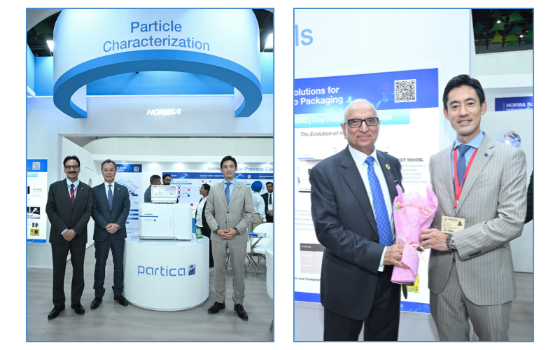
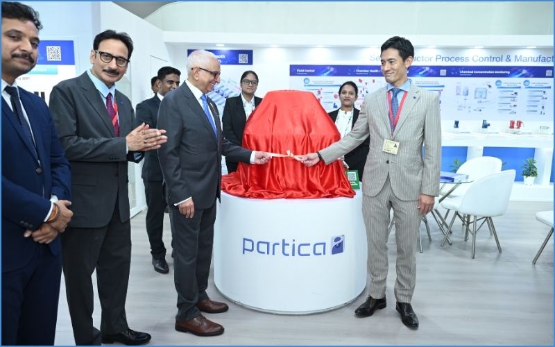
PARTICA Unveiled for Advanced Particle Characterization
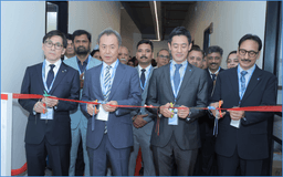
One of the key highlights of HORIBA’s participation was the unveiling of PARTICA, HORIBA’s advanced particle characterization solution.
Particle characterization plays an important role in semiconductor materials research and manufacturing, where understanding particle size and material characteristics can contribute to process optimization, quality control and consistency.
Through PARTICA and HORIBA’s broader material-characterization portfolio, visitors were introduced to technologies designed to support accurate measurement and analysis across semiconductor and advanced-material applications.
The unveiling further strengthened HORIBA’s proposition of connecting analytical capabilities used in laboratories and R&D environments with the requirements of advanced semiconductor manufacturing.
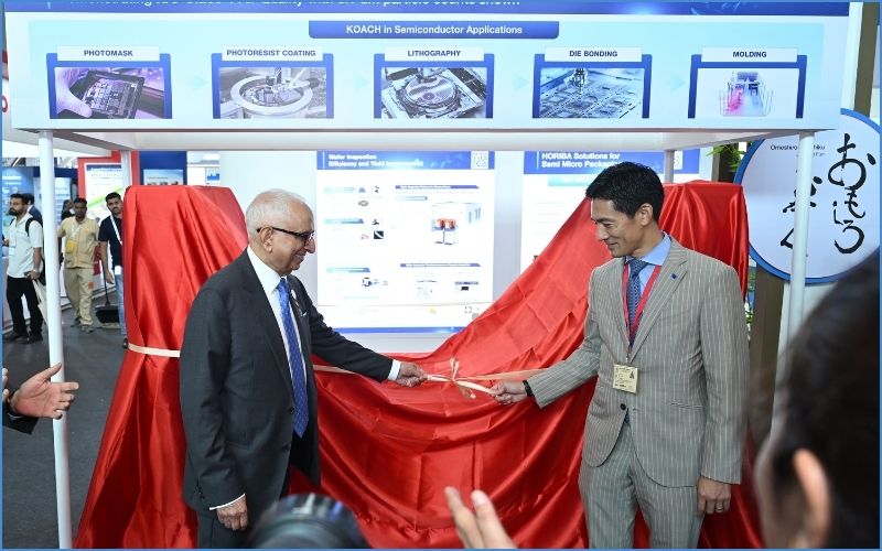
Advancing Cleanroom and Contamination Control
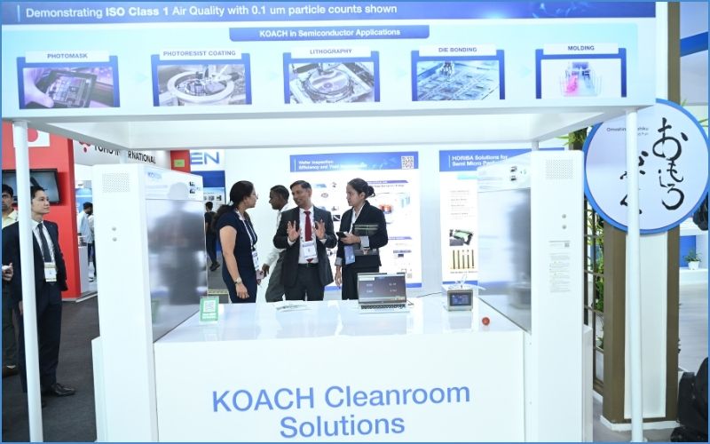
HORIBA India also introduced its Cleanroom Solutions, highlighting the growing importance of contamination control within semiconductor manufacturing environments.
As semiconductor structures become increasingly complex and manufacturing tolerances become tighter, controlling airborne particles and maintaining highly controlled production environments are critical to manufacturing quality and process reliability.
HORIBA’s cleanroom solutions are designed to support high-purity manufacturing environments and complement its broader semiconductor portfolio covering process monitoring, material analysis and manufacturing infrastructure.
The showcase demonstrated how HORIBA can support customers not only at individual measurement points but across different stages and environments within semiconductor production.
Demonstrating HORIBA’s “Lab to Fab” Capabilities
A key theme of HORIBA’s presence at SEMICON India 2026 is its “Lab to Fab” approach — connecting scientific analysis and material characterization with technologies required within semiconductor fabrication and production environments.
Visitors to the HORIBA booth are able to explore solutions across areas including:
- Material Characterization
- Chemical Concentration Monitoring
- Process Monitoring and Endpoint Detection
- Fluid and Mass Flow Control
- Reticle and Mask Inspection
- Semiconductor Manufacturing Facility Solutions
- Automated Thin-Film Inspection
- ISO Class 1 Cleanroom Solutions
Through live demonstrations and interactions with HORIBA experts, the showcase provides a broader perspective on how measurement, analysis and process-control technologies work together across the semiconductor manufacturing ecosystem.
Enabling Precision Across Semiconductor Manufacturing
HORIBA has a longstanding presence in analytical and measurement technologies supporting semiconductor applications, including precise gas and liquid mass-flow control, chemical and gas monitoring, process analysis, material characterization and inspection.
At SEMICON India 2026, these capabilities are being presented as an integrated portfolio aimed at addressing challenges across research, process development, manufacturing and quality control.
The first day also provided a platform for meaningful conversations with customers, semiconductor industry experts, academia, researchers and technology partners on topics ranging from advanced materials and contamination management to process precision and the future requirements of semiconductor manufacturing in India.
These interactions reflect the broader purpose of SEMICON India — bringing government, industry, academia, startups and the global semiconductor ecosystem together to strengthen collaboration and accelerate the development of India’s semiconductor value chain.
Supporting India’s Semiconductor Growth Journey
India’s semiconductor ecosystem is entering an important phase of development, creating opportunities across materials, equipment, fabrication, packaging, electronics manufacturing, research and supporting infrastructure.
For HORIBA India, participation in SEMICON India 2026 represents an opportunity to bring together global semiconductor expertise and local capabilities while working closely with customers and ecosystem partners to address emerging requirements.
Through advanced analytical technologies, process-control solutions and manufacturing-environment capabilities, HORIBA aims to contribute to an ecosystem where precision, reliability, innovation and sustainability support the next generation of semiconductor technologies.
The strong engagement on the opening day of SEMICON India 2026 has set the stage for continued discussions and technology demonstrations throughout the three-day event.
Visit HORIBA India at Hall 1, Booth 224, Yashobhoomi (IICC), New Delhi, from 17–19 September 2026 to experience HORIBA’s “Lab to Fab” semiconductor solutions.
Together, we are advancing precision and innovation for the future of semiconductor technology.